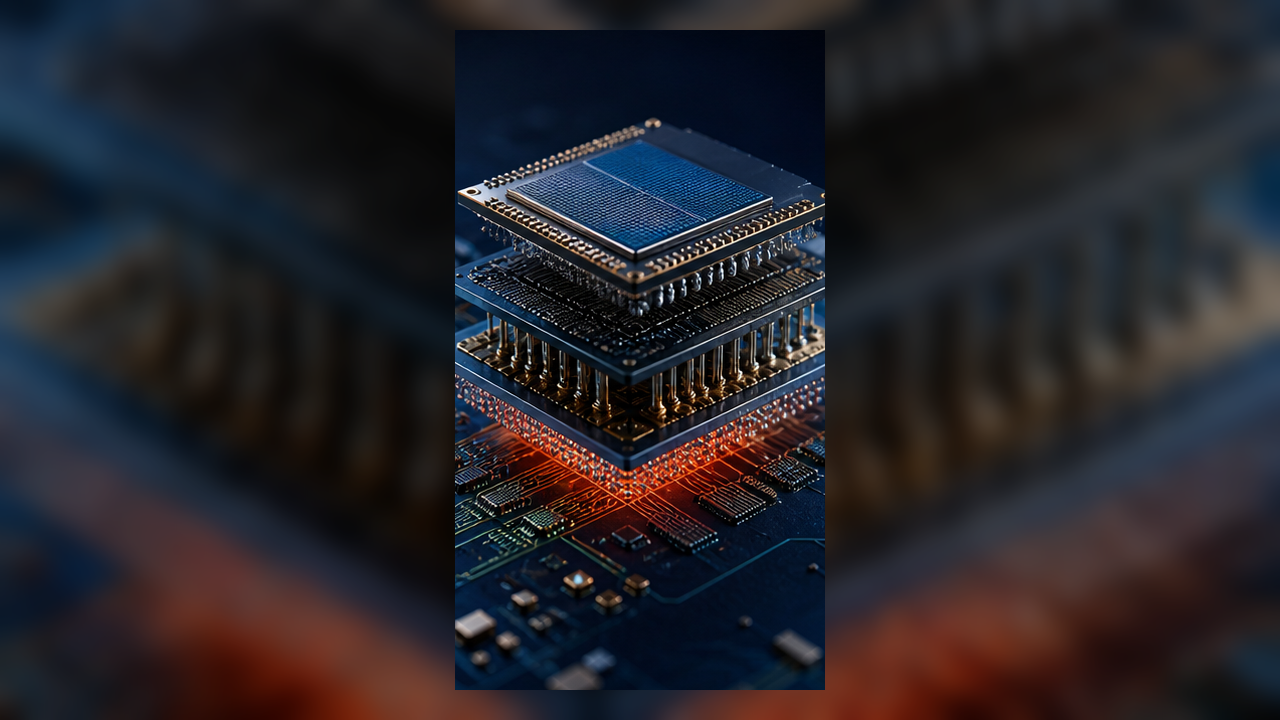
The semiconductor supply chain can produce a wafer and still fail to deliver an AI accelerator. The missing step is often advanced packaging: combining compute dies, high-bandwidth memory, substrates, and power delivery into a system that can be tested and shipped. As AI systems become larger, packaging is becoming a strategic manufacturing capability rather than a final assembly detail.
More dies create more coordination
Chiplets improve flexibility and yield, but they also make the package more complex. The designer must align electrical connections, thermal behavior, memory bandwidth, and test coverage across several pieces of silicon. A package that works in a laboratory may still be difficult to manufacture at volume.
This is why capacity expansion must include packaging materials and equipment. Interposers and substrates have their own production limits, while HBM stacks require specialized manufacturing and testing. A shortage in any one layer can hold back the complete accelerator.
The industry response
Foundries, outsourced assembly and test companies, memory suppliers, and substrate vendors are all investing in capacity. The goal is not only more square meters of factory space; it is higher throughput with predictable yields. Standardized interfaces can make the ecosystem more flexible, but they do not remove thermal and validation challenges.
For AI buyers, the practical lesson is to ask for system-level availability. A vendor's GPU announcement is not the same as a shipping product. Lead time, memory configuration, networking, and service capacity determine whether a model can be deployed on schedule.