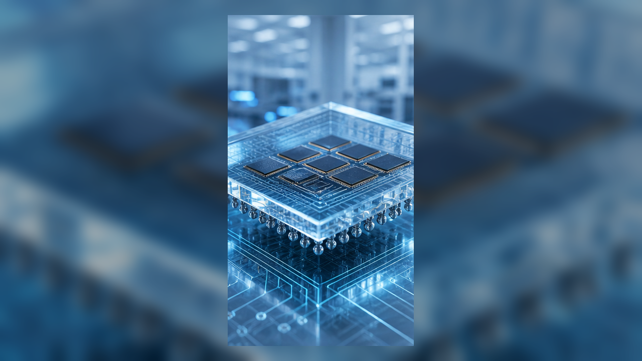
Intel's collaboration with Lens Technology around advanced packaging is a reminder that AI-chip scaling is not only about smaller transistors. Packaging materials, substrate quality, thermal behavior, and interconnect density are becoming central constraints.
Large AI accelerators are built as systems of compute die, memory stacks, substrates, interposers, and high-speed links. As packages grow larger and more power dense, traditional materials face mechanical and electrical limits. That is why glass and other advanced substrate approaches are drawing more attention.
The opportunity is higher signal integrity, better dimensional stability, and new ways to route dense interconnects. The challenge is manufacturability. A material that works in a demonstration must still survive yield, cost, tooling, and volume requirements.
Advanced packaging has become the bridge between chip design and system design. The companies that control that bridge can influence how much AI compute fits inside a rack, a power budget, and a delivery schedule.